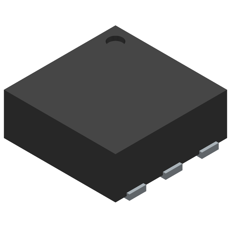
Low quiescent current (5µA) boost converter, featuring 15nA bypass operation. This integrated circuit offers a maximum output current of 700mA with a minimum output voltage of 3.3V. Operating from a minimum input voltage of 900mV up to 5V, it supports a single positive output. The device is housed in a SON package, suitable for surface mounting, and operates within a temperature range of -40°C to 85°C. This RoHS compliant component utilizes a synchronous rectifier and a boost topology.
PackageSON
MountingSurface Mount
Quick Jump:
Technical Specifications
Texas Instruments TPS61291DRVR technical specifications.
General
| Package/Case | SON |
| Lead Free | Lead Free |
| Max Input Voltage | 5V |
| Min Input Voltage | 900mV |
| Max Operating Temperature | 85°C |
| Min Operating Temperature | -40°C |
| Max Output Current | 250mA |
| Min Output Voltage | 3.3V |
| Mount | Surface Mount |
| Number of Outputs | 1 |
| Operating Supply Voltage | 5V |
| Output Configuration | Positive |
| Output Current | 700mA |
| Packaging | Tape and Reel |
| Quiescent Current | 5uA |
| Radiation Hardening | No |
| RoHS Compliant | Yes |
| Synchronous Rectifier | Yes |
| Topology | Boost |
Compliance
| RoHS | Compliant |
Datasheet
Texas Instruments TPS61291DRVR Datasheet
Download the complete datasheet for Texas Instruments TPS61291DRVR to view detailed technical specifications.
This datasheet cannot be embedded due to technical restrictions.
Product Images

