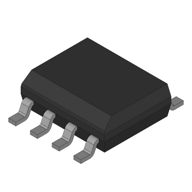
FDS6672A

FDS6672A

onsemi

Description:

Trans MOSFET N-CH 30V 12.5A 8-Pin SOIC N T/R

Country of Origin:

China

Introduction date:

Mar 8, 2000

Updated:+90 days

Overview

Familiarize yourself with the fundamental general information, properties, and characteristics of the component, along with its compliance with industry standards and regulations.

LifeCyclePremium
EU RoHS Yes
RoHS Version2011/65/EU, 2015/863
Category Path
Semiconductor > Diodes, Transistors and Thyristors > FET Transistors > MOSFETs

Datasheet

Get a comprehensive understanding of the electronic component by downloading its datasheet. This PDF document includes all the necessary details, such as product overview, features, specifications, ratings, diagrams, applications, and more.

Manufacturing

The manufacturing information specifies the technical requirements and specifications for producing and assembling the component. This information is crucial for manufacturers to maintain the quality and reliability of the components, and ensure they are compatible with other devices and components.

Reflow Temp. Source
Number of Wave Cycles

Parametric

The parametric information displays vital features and performance metrics of the component, which helps engineers and supply chain managers to compare and choose the most appropriate electronic component for their applications and needs.

Product Line
Breakdown Voltage Type
Minimum DC Current Gain
Typical Switch Charge
Typical Gate Resistance
Typical Reverse Recovery Charge
Typical Forward Transconductance
Tradename
Minimum Gate Threshold Voltage
Typical Reverse Transfer Capacitance @ Vds
Maximum Offset Voltage
Maximum Positive Gate Source Voltage
Minimum Gate Resistance
Maximum Gate Resistance
Typical Gate Threshold Voltage
Typical Diode Forward Voltage
Maximum Diode Forward Voltage
Typical Reverse Recovery Time
Maximum Pulsed Drain Current @ TC=25°C
Maximum Forward Transconductance
Minimum Forward Transconductance
Minimum IDSS
ID For GFS
VDS For GFS
Maximum Input Capacitance @ Vds
Typical IDSS
Maximum Storage Temperature
Operating Junction Temperature
Maximum Gate Source Leakage Current
Minimum Storage Temperature
Typical Gate to Drain Charge
Typical Gate to Source Charge
Maximum Junction Ambient Thermal Resistance
Maximum Junction Case Thermal Resistance
Typical Fall Time
Typical Rise Time
Typical Turn-Off Delay Time
Supplier Temperature Grade
Typical Turn-On Delay Time
Configuration
Maximum Absolute Continuous Drain Current
Category
Channel Mode
Channel Type
Number of Elements per Chip
Process Technology
Maximum Drain Source Voltage
Maximum Gate Source Voltage
Maximum Continuous Drain Current
Material
Maximum Gate Threshold Voltage
Maximum Drain Source Resistance
Maximum IDSS
Typical Gate Charge @ Vgs
Typical Gate Charge @ 10V
Typical Input Capacitance @ Vds
Maximum Power Dissipation
Minimum Operating Temperature
Maximum Operating Temperature
Typical Output Capacitance

CAD Models

Access 3D CAD models, symbols, and footprints of the component. Visualize its structure and dimensions, integrate designs, and optimize performance effortlessly.

Crosses

Interested in More Free Data?

Discover a form-fit-function equivalent from another manufacturer or even suitable upgrades and downgrades, and much more.

Go Premium

No Credit Card. No Commitment.