2-output, 1-input clock fanout buffer operating up to 250MHz. Features LVCMOS input and gold contact plating. Surface mountable in a 8-pin TSSOP package with dimensions of 4.5mm length, 3.1mm width, and 1.05mm height. Operates from a 2.3V to 3.6V supply voltage with a maximum supply current of 10mA. RoHS compliant with a propagation delay of 2.6ns.
Frequency250MHz
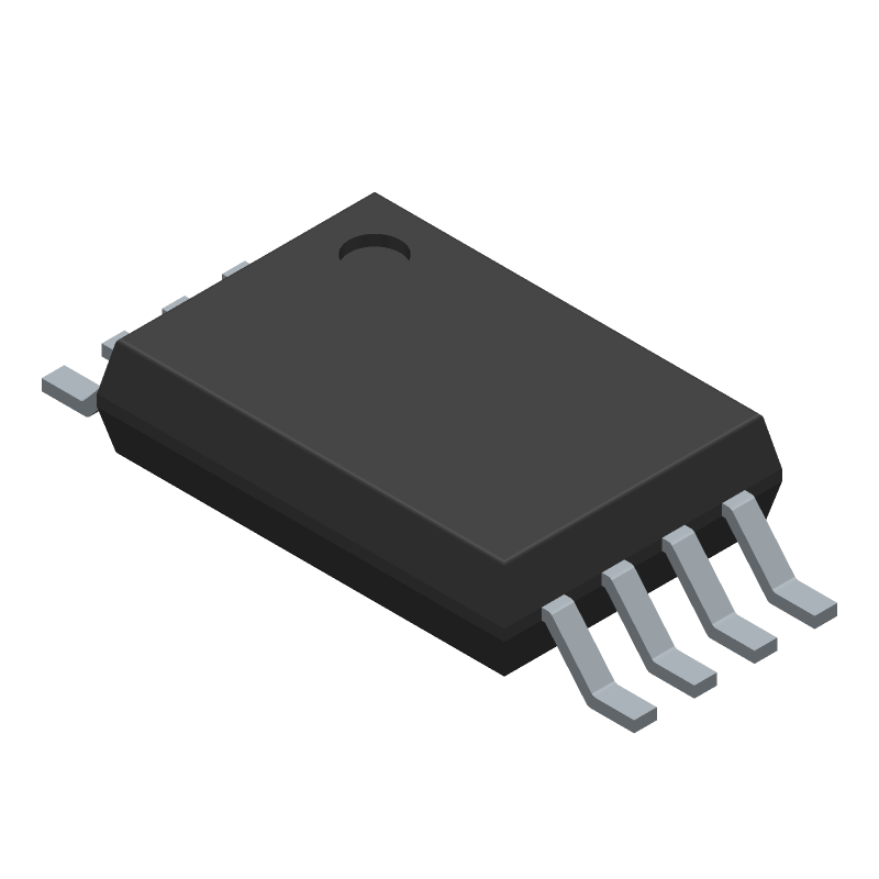
PackageTSSOP
Current6mA
MountingSurface Mount
Quick Jump:
Technical Specifications
Texas Instruments CDCLVC1102PW technical specifications.
General
| Package/Case | TSSOP |
| Contact Plating | Gold |
| Frequency | 250MHz |
| Height | 1.05mm |
| Input | LVCMOS |
| Lead Free | Lead Free |
| Length | 4.5mm |
| Max Frequency | 250MHz |
| Max Operating Temperature | 85°C |
| Min Operating Temperature | -40°C |
| Max Supply Current | 10mA |
| Max Supply Voltage | 3.6V |
| Min Supply Voltage | 2.3V |
| Mount | Surface Mount |
| Number of Circuits | 1 |
| Number of Outputs | 2 |
| Package Quantity | 150 |
| Packaging | Rail/Tube |
| Propagation Delay | 2.6ns |
| Radiation Hardening | No |
| Reach SVHC Compliant | No |
| RoHS Compliant | Yes |
| Supply Current | 6mA |
| Turn-On Delay Time | 10ns |
| Width | 3.1mm |
Compliance
| RoHS | Compliant |
Datasheet
Texas Instruments CDCLVC1102PW Datasheet
Download the complete datasheet for Texas Instruments CDCLVC1102PW to view detailed technical specifications.
This datasheet cannot be embedded due to technical restrictions.
Product Images
